Soan Papdi FPGA
Most FPGA boards are designed for experienced engineers. You spend hours hunting for components, wiring up circuits, and debugging setups before writing a single line of code.
Soan Papdi is different.
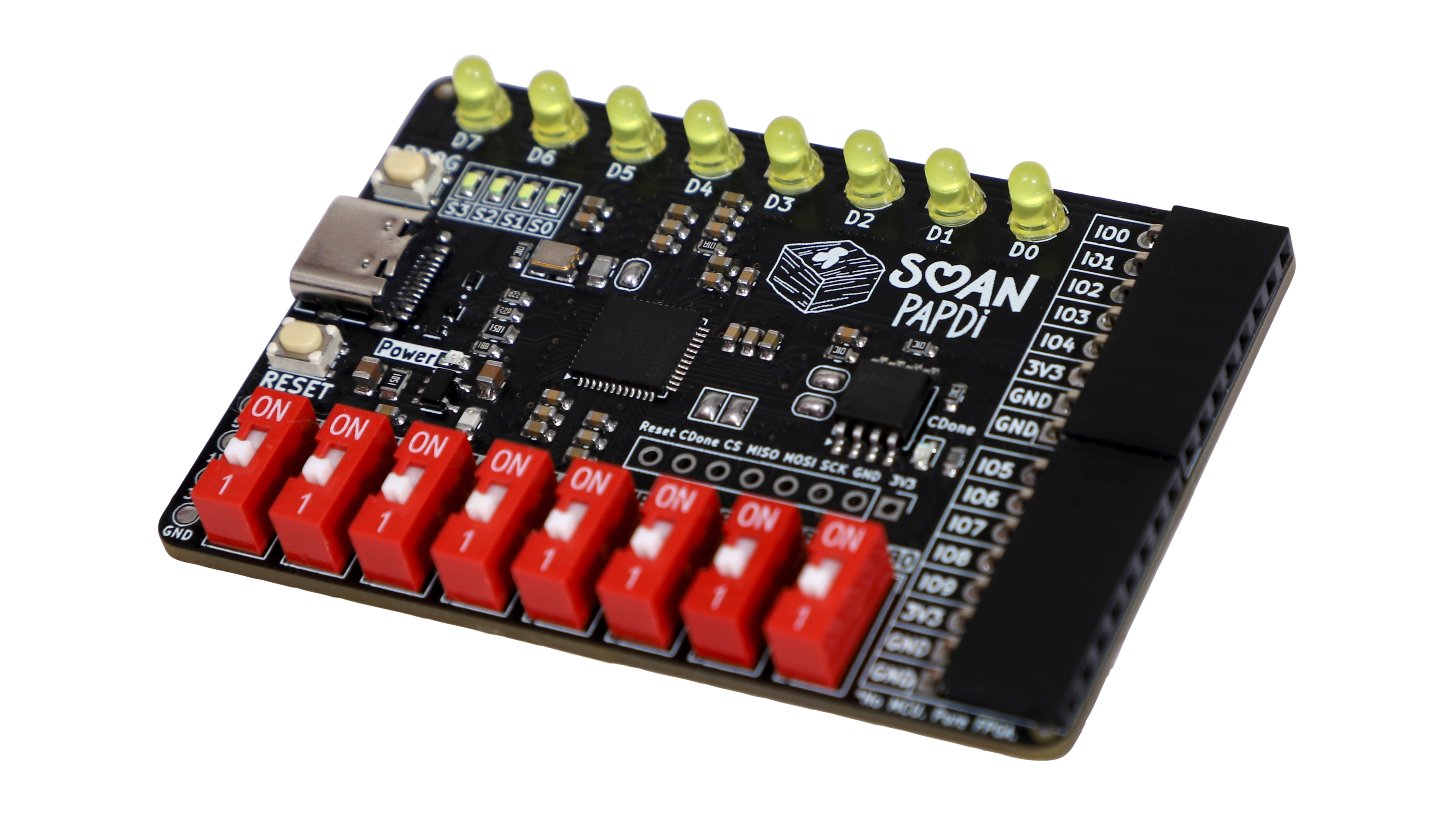
Soan Papdi is a beginner-friendly FPGA development board with everything you need onboard — LEDs, switches, and GPIO headers — so you can start learning digital design immediately, without the usual hardware setup headaches.
No complex HDL needed
No complicated installation flow. No lame driver installation. Download the IDE, double click, get started!
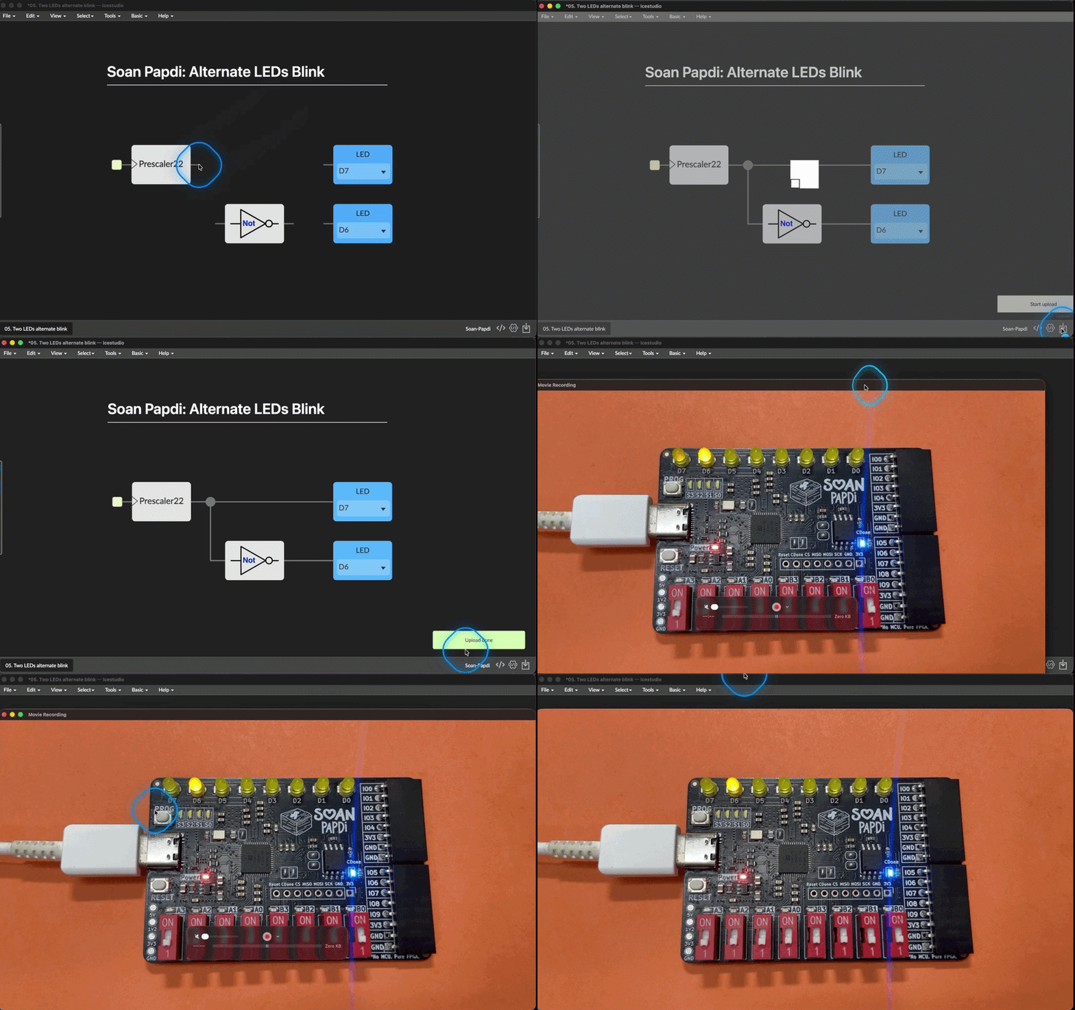
Program it using the open-source iCEStudio IDE or use RAW HDL!
Specification
- FPGA: Lattice iCE40UP5K FPGA
- Datasheet: Link
- Logic Resources: 5,280 LUTs (capable of hosting RISC-V soft-core CPUs)
- Embedded Memory: 120 Kbit Block RAM
- SPRAM: 1 Mbit (128 KB) Single-Port SPRAM
- Clocking: On-chip PLL
- Hard IP: 2 × SPI, 2 × I²C
- Internal Oscillators: 10 kHz and 48 MHz
- DSP Resources: 8 × DSP multiplier blocks
- Onboard Storage: 128 Mbit onboard SPI Flash
- User Interface:
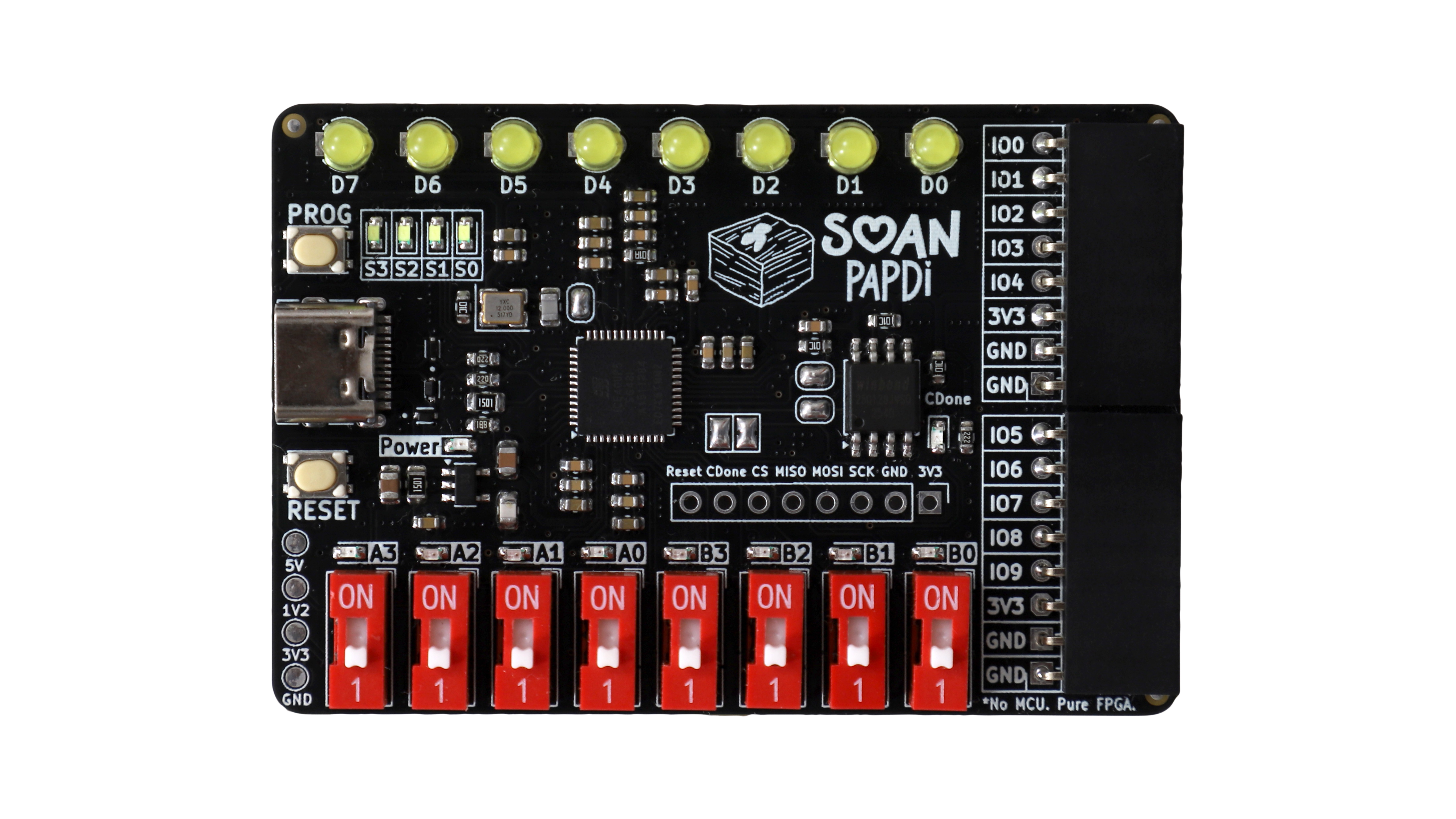
- 8 × yellow 3.0 mm through-hole LEDs (D7–D0)
- 4 × white 0603 SMD status LEDs (S3–S0)
- 8 × DIP switches with orange SMD indicator LEDs
- 2 × push buttons (Program & Reset)
- 10 × I/O pins for external sensors & peripherals
- USB: USB-C, fully controlled by FPGA (no external MCU)
- Programming: DFU bootloader (preloaded)
- Toolchain Support: iCE Studio, APIO, Yosys, nextpnr, IceStorm, Icarus Verilog, Amaranth HDL
- Power: USB-5V
- Dimension: 67.5 x 45.5 mm
- Platform: Works on Windows, macOS & Linux
Pin Diagram
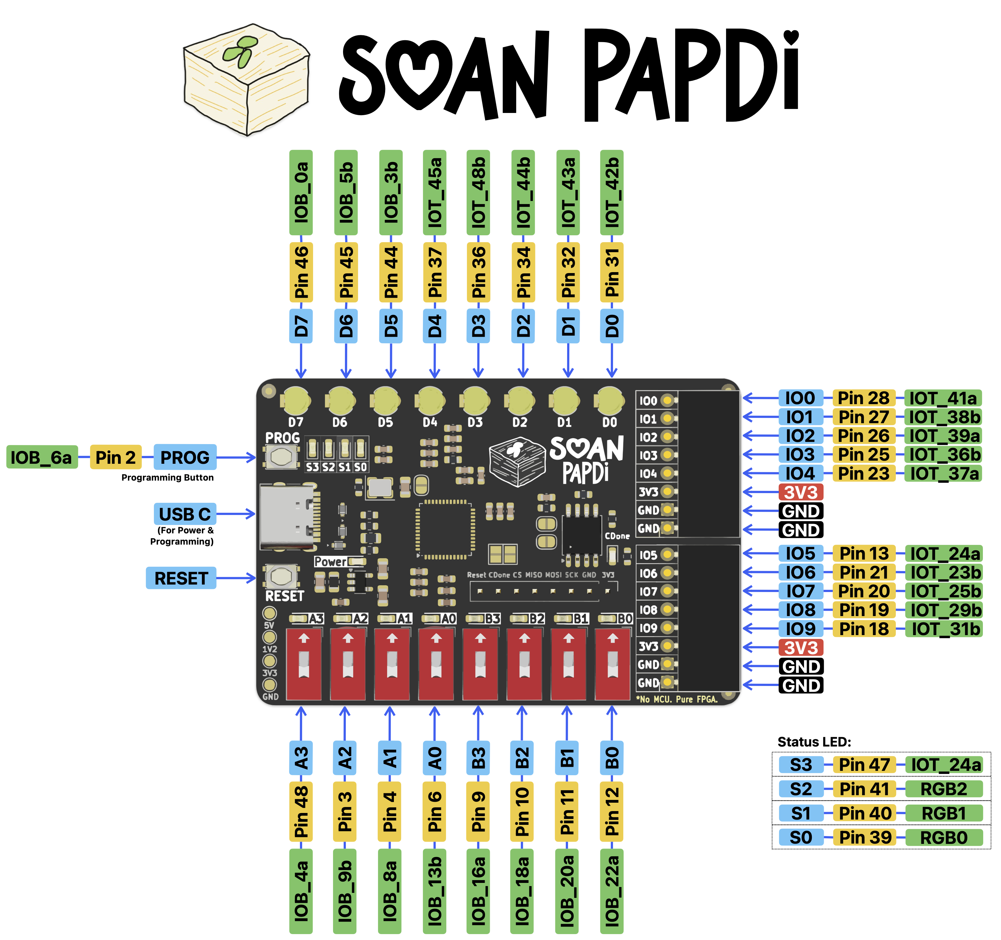
Why this design ?
Soan Papdi is designed for learning — every component has a reason.
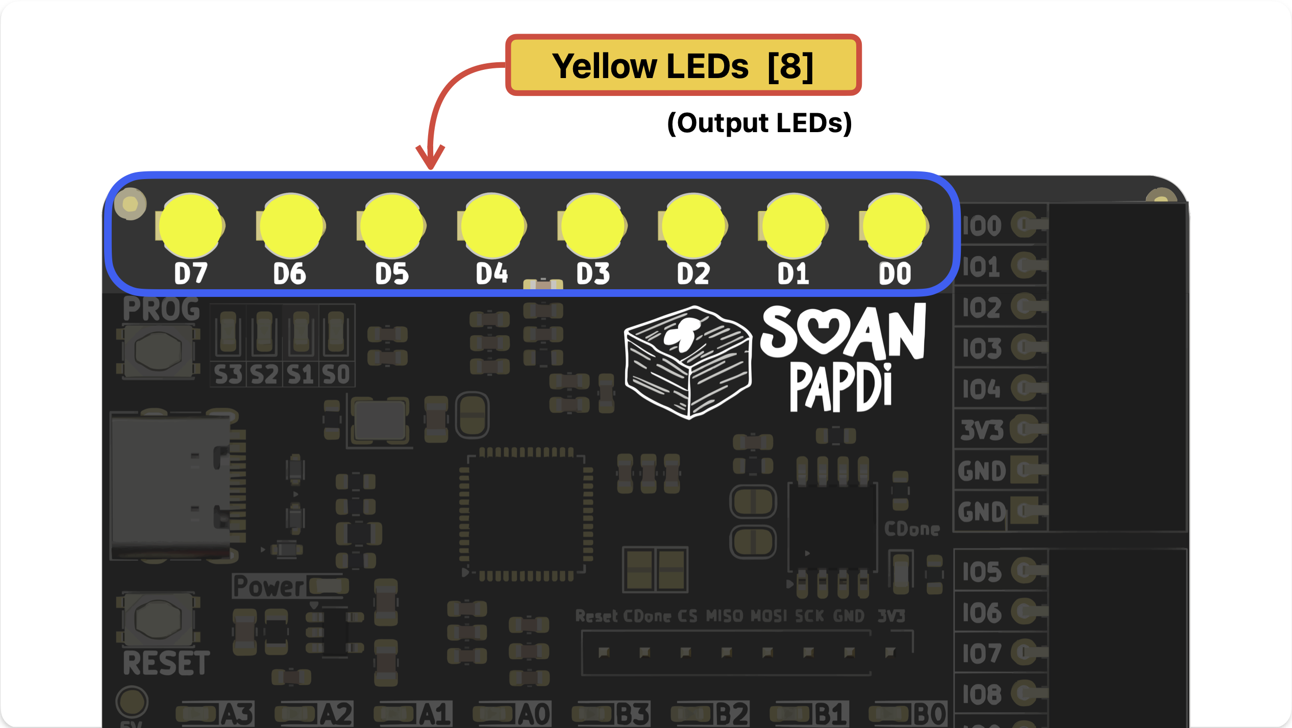
Output LEDs (D7–D0)
On top, we have 8 output LEDs. (D7 to D0) These aren’t random. We chose 8 yellow LEDs because 8-bit data is fundamental to digital systems.
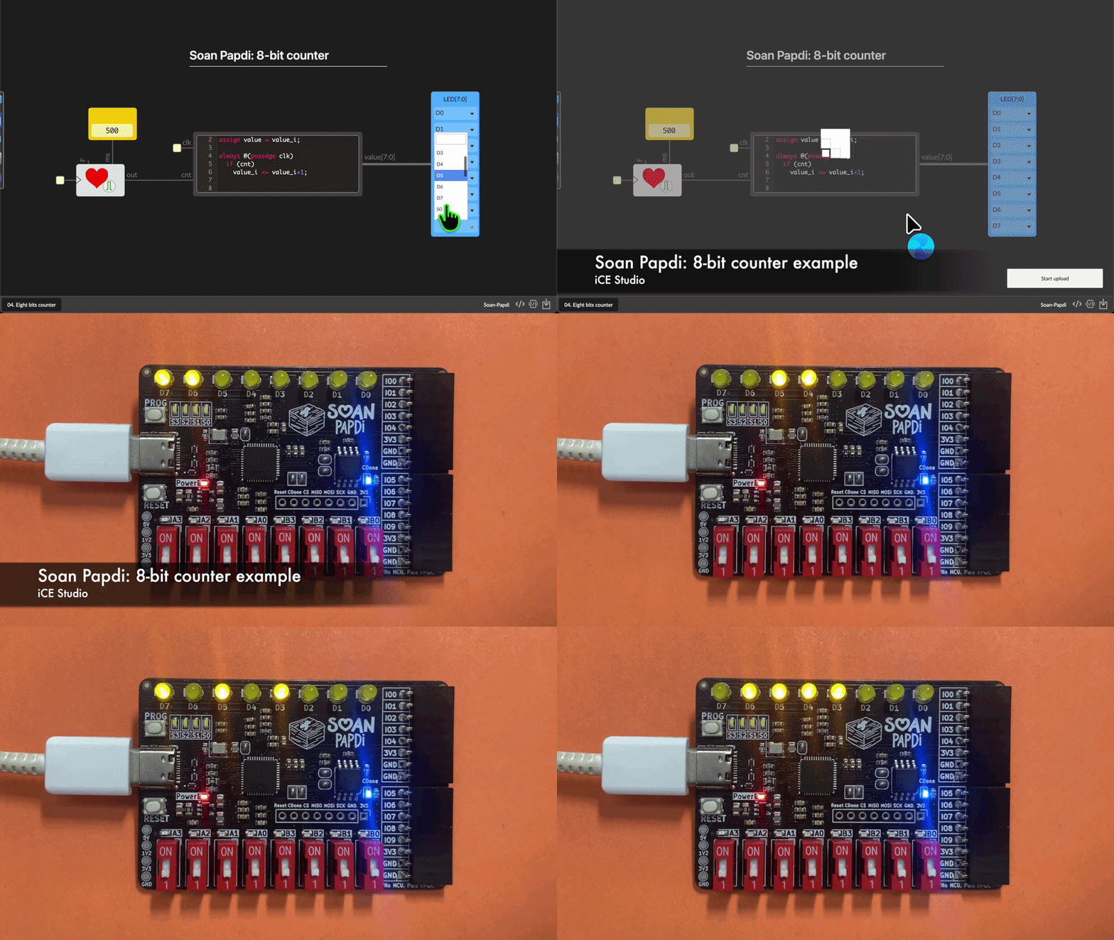
When you build things like counters, shift registers, state machines, or simple processors, you can visualize the output directly on the LEDs in real time.
Status LEDs (S3–S0)
Right next to the output LEDs are 4 white LEDs for status signals.
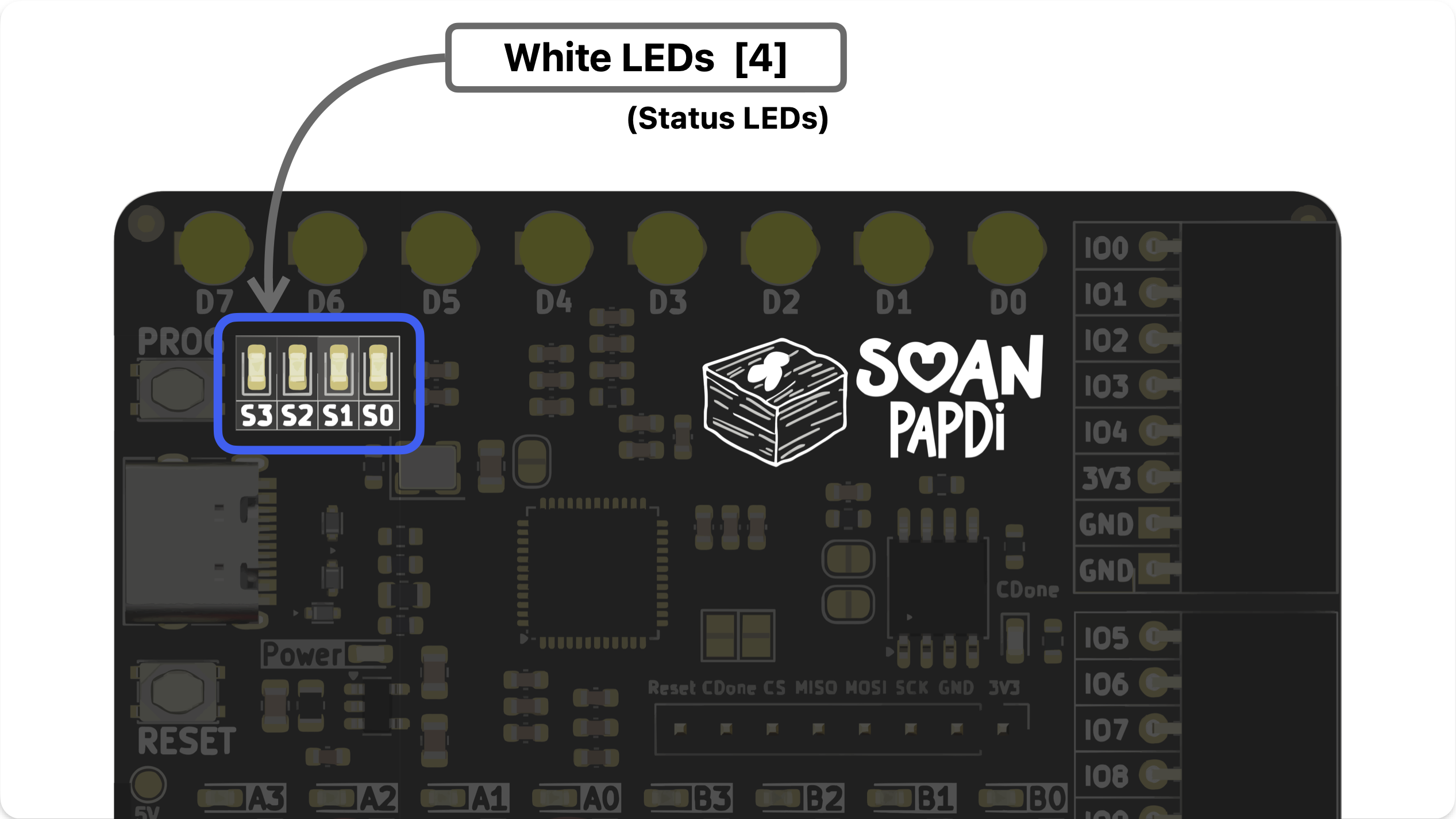
Use them for carry flags, overflow indicators, error signals, or any custom status output — so you can see exactly what’s happening inside your circuit at a glance.
Input Switches (A3–A0 & B3–B0)
At the bottom side of the board we have two sets of switches:
- Set A: A3 to A0
- Set B: B3 to B0
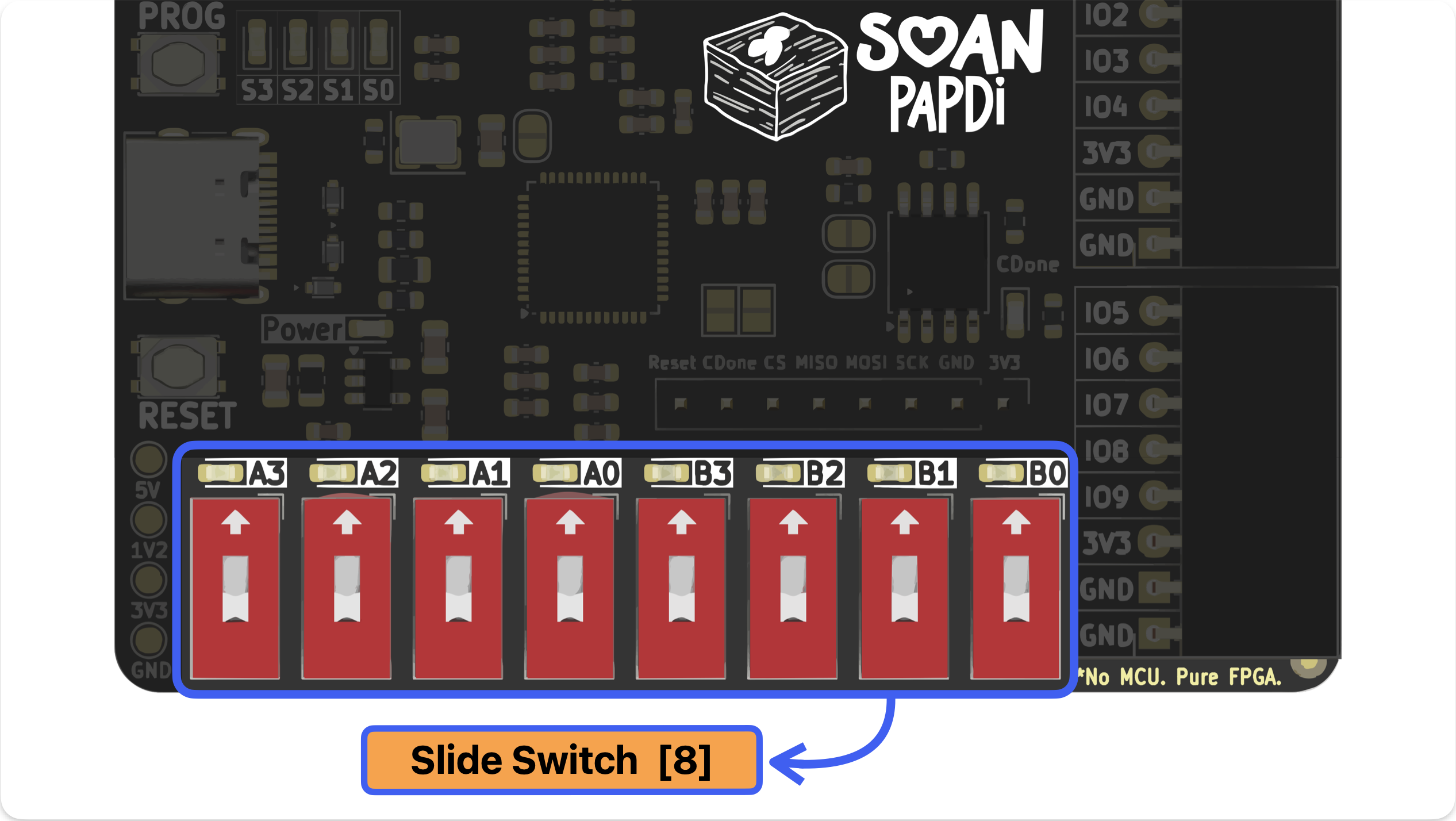
These switches let you input two 4-bit values directly into your FPGA design.
Build an adder, subtractor, comparator, or simple calculator, then change the inputs and observe the results instantly on the LEDs.
From experimenting with combinational logic to debugging larger designs, the switches provide a simple and intuitive way to interact with your hardware.
GPIO Pins (IO0–IO9)
On the right side of the board we have 10 GPIO pins that let you go beyond the onboard peripherals.
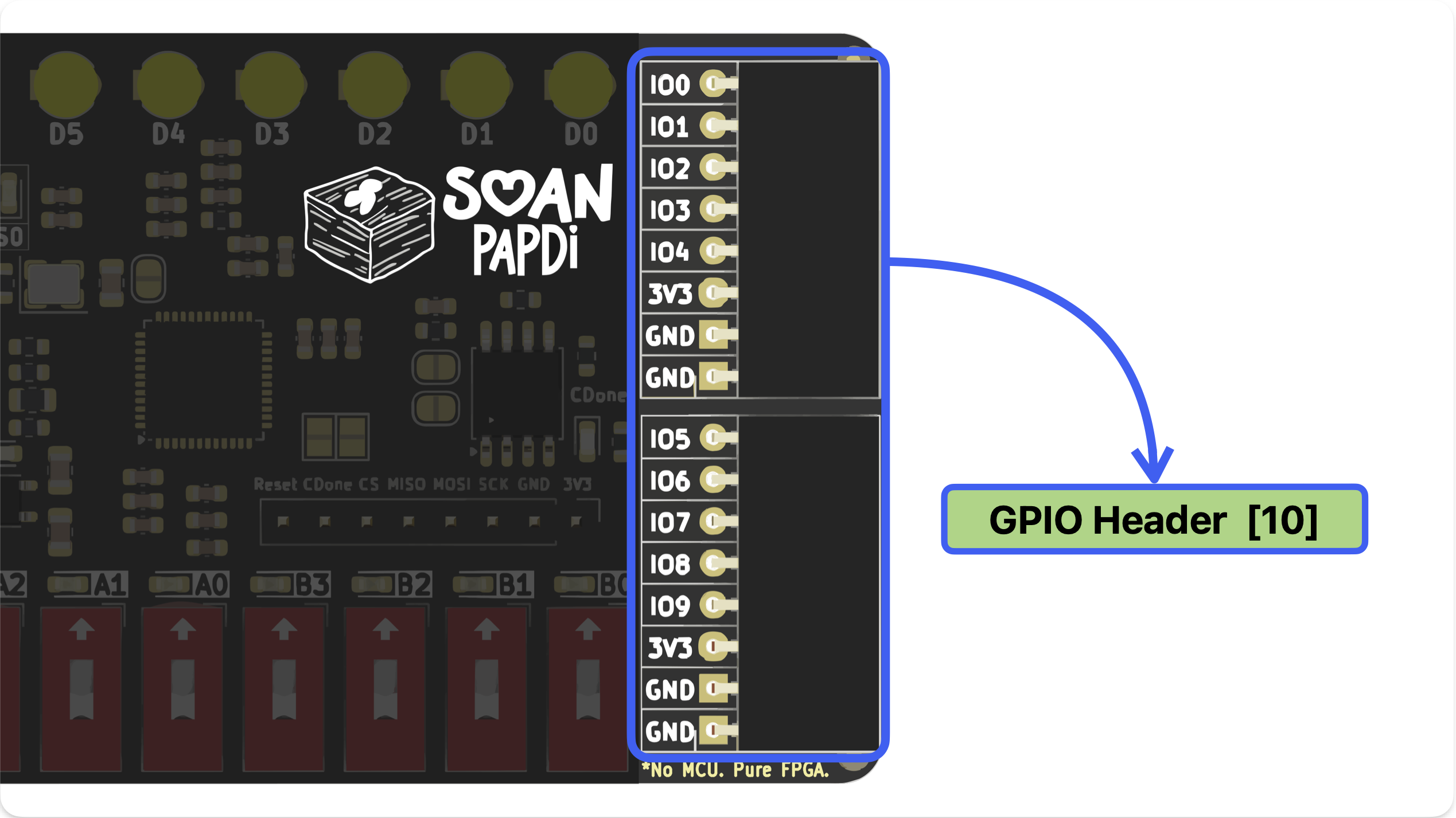
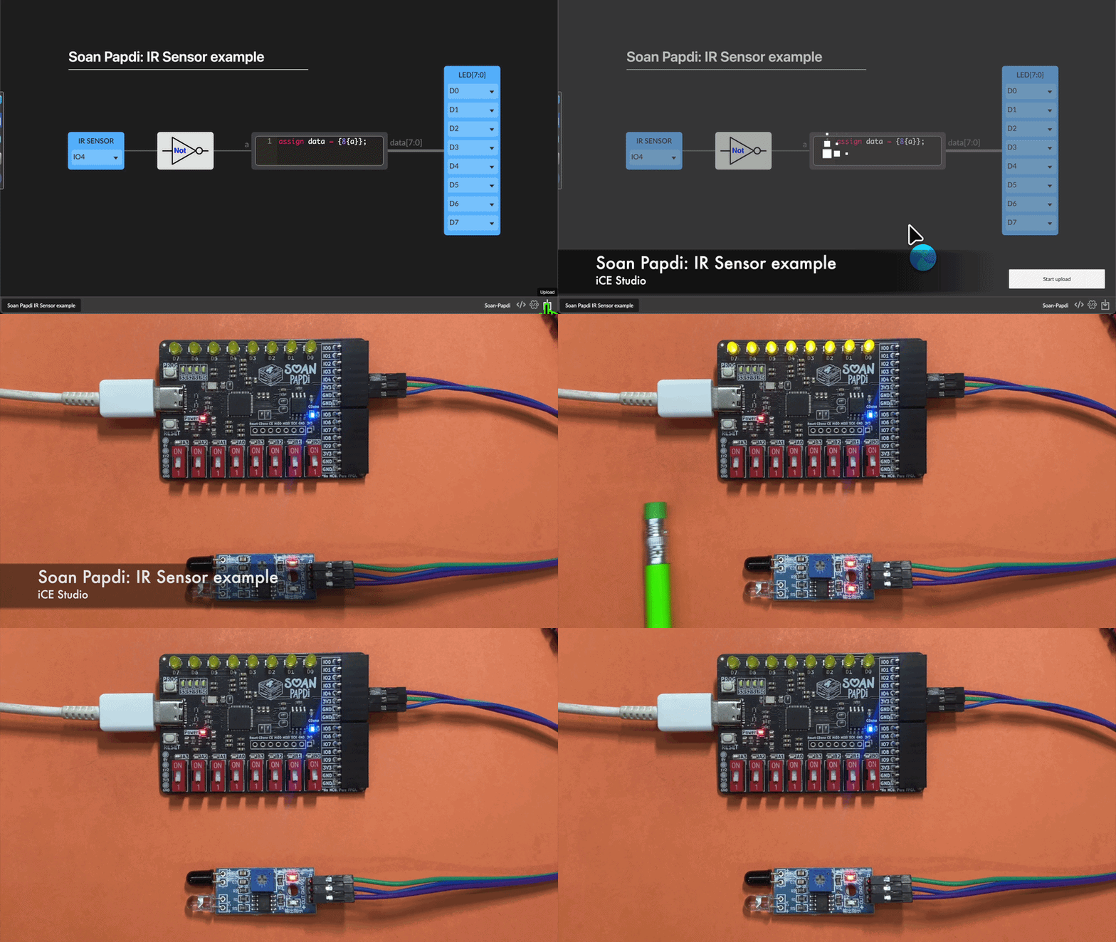
Connect sensors, displays, motors, communication modules, or your own custom hardware to extend the capabilities of Soan Papdi.
Why We Made Soan Papdi ?
FPGAs are incredibly powerful—but getting started can be painful.
Too complex. Too many tools. Too many things that can go wrong. And that’s exactly where many people give up.
One day, Piyush and Hardik were discussing this problem. At some point he asked: “What if we built our own FPGA board?”
Not another board for experts, but something designed for people who just want to start.
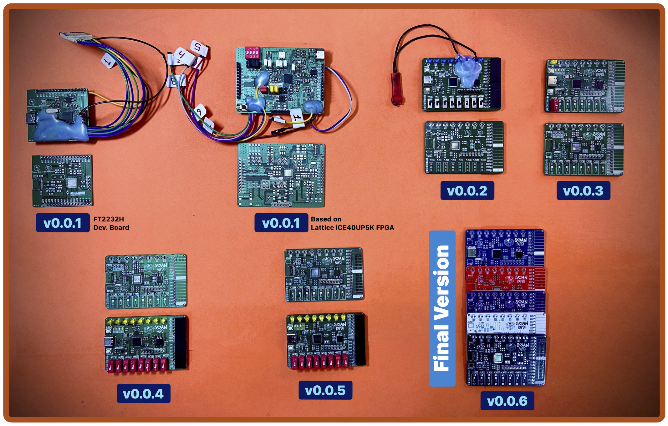
That simple question started a ten-month journey of designing, testing, and refining the board through multiple hardware iterations and real user feedback.
Learning Resources
To make things easier, Piyush Itankar has created a Digital Electronics 101 course, where everything is explained step by step.
Start learning here: Soan Papdi FPGA 101 Course by Piyush
You can explore built-in examples and learn by doing.

Start simple — build basic gates like AND, OR, or a decoder.
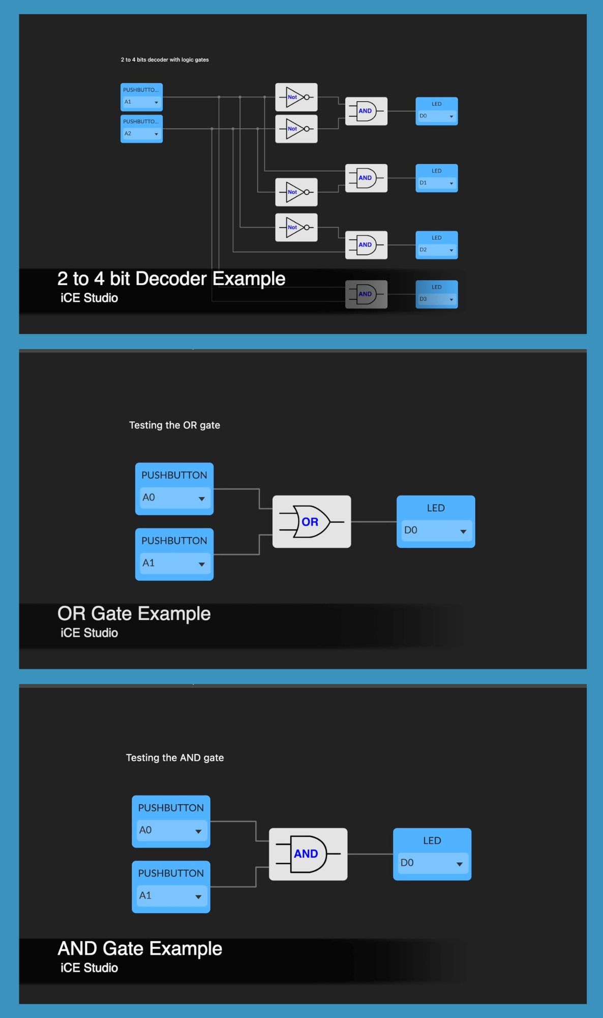
Once you’re comfortable with the basics, move on to these advanced projects:
- RISC-V CPU — A RISC-V processor implementation
- Z80 CPU — A recreation of the classic Z80 processor
- Hack CPU — The Nand2Tetris Hack CPU, built gate by gate
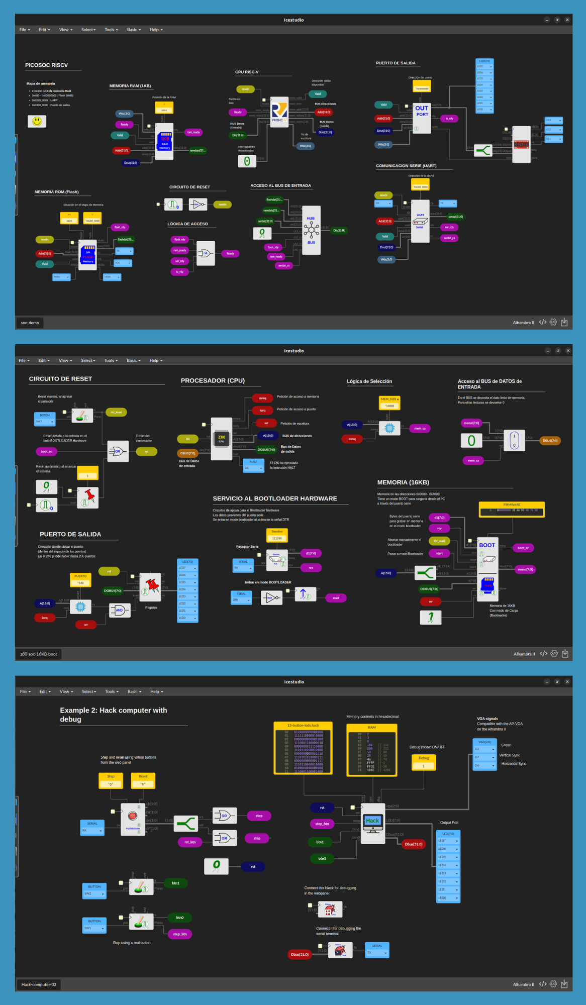
Looking for more inspiration?
Browse the full iCEstudio Example Collection for additional projects organized by category.
Interested in This Project?
You can sign up at the top of this page to be notified when the campaign launches and to receive other updates. We only send out relevant content, and you can unsubscribe at any time.
The Team
Proposal of Soan Papdi was made by Piyush, the idea was brought to life by Hardik & Lakshya.

Hardik Seth
Embedded Engineer
STEMpedia
LinkedIn · X · YouTube
Engineer by day, Maker by night - playing with electronics since the age of 9. From childhood, I’ve loved tearing things apart, rebuilding them, and learning through hands-on experimentation and how-to videos.
Currently working as embedded engineer who designs PCBs, writes firmware, and enjoys turning ideas into complete, working hardware products from first schematic to final blink.

Piyush Itankar
Senior Embedded SW Engineer
Google | Ex-Intel
LinkedIn · X · YouTube
Electrical Engineer holding a Master’s degree in Embedded Systems, with a proven track record at industry giants. At Intel, contributed expertise to Navigation Firmware, Bluetooth Driver development, and RF validation software.
Currently thriving as an Embedded Software Engineer at Google, drove innovation in Firmware development for the Power Management Sub-system on Tensor SoCs (Pixel Phones) and presently advancing system software for the Pixel Watch.

Lakshya Seth
Digital Craftsman
Class 12th student
LinkedIn · YouTube
Love to build things, breaking and tearing things apart, to really learn how it’s working, and what I can build with it. I like to play with Arch Linux and electronics.
Currently, I’m in 12th grade and trying to get into an engineering college.